 Door: myProto - online PCBA prototypes en series
By applying Pin-in-Paste (PIP) reflow technology it is possible to solder THT components with a reflow oven. The successful application of this technology saves time and therefore money. myProto spoke with Tom Meeus of Rotec, specialist in stencils and pastes, about this technology and what you need to consider in order to apply this technology successfully.
THT and SMD components in 1 process step
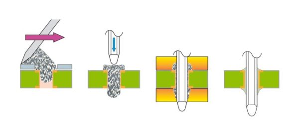
Pin-in-Paste technology is the name of the process in which through-hole components are soldered via reflow technology. Sufficient paste is applied through the stencil to provide the joint with solder. Subsequently, the THT component can be placed manually or mechanically, after which the reflow oven fuses all solder joints together. As standard, these components are mounted via wave soldering, selective soldering or hand soldering.
Tom Meeus: �The advantage of PIP is that through-hole components are soldered together with SMD components in 1 process step. Because one process step is saved, usually wave or hand soldering, PIP is therefore a cheaper and faster way of production. Especially when a design consists mostly of SMD components and only a few best before date, it is very interesting to apply PIP technology. An additional advantage is that THT components with a small pitch can be soldered better using this method. �
Not all THT components are suitable for Pin-In-Paste
A lot of time can therefore be gained by applying PIP technology. But if you want to use this technology, it is important to choose THT components that are suitable for this technology. Tom Meeus sees two important conditions: temperature and stand-off.
�The peak temperature of a standard lead-free oven profile can quickly rise to 250 degrees C, so potential THT components must be able to handle that temperature. If this is not the case, one can also switch to low-melt solder paste. With this one can lower the solder peak to 180 to 200C. This must be considered on a case-by-case basis because not every application allows low-melt soldering.
In addition, it is wise not to introduce too much heat into the PCB during assembly. Due to excessive heating, the viscosity of solder paste will quickly decrease, so there is the risk that part of the paste will drip into the oven. The result is irregular solder volume and contamination of the reflow oven. That is why we propose a fairly moderately linear solder profile that does not rise quickly, especially in the first zones. Besides, it is important that the PIP component has a certain stand-off. This is the distance between the PCB and the bottom of the component body. This stand-off ensures that there is space between the PCB and the component to apply sufficient solder paste. We recommend a stand-off of at least 0.5mm. ��
PCB Layout for Pin-In-Paste
If you want to apply PIP, it is wise to apply adapted design rules from the design phase. Tom Meeus: �An important parameter is the ratio between the diameter of the pin and the diameter of the borehole in the PCB. This determines the amount of solder needed to fill the hole plus the meniscus or reflow towards the pen. It is therefore a very important parameter because solder paste consists of half of flux by volume and half of metal powder. If you choose a relatively large hole, the component will be easy to place by an operator or possibly by machine. But you need a large volume of paste to solder everything neatly according to the applicable IPC standards. That is why it is better not to follow the standard wave solder design rules because they use relatively large pin / hole ratios, but it is better to choose an adapted PIP design from the design phase. MyProto can provide the necessary advice here! ��
Custom stencil design for Pin-In-Paste technology
Tom Meeus: �You can use a fairly simple formula to calculate the paste volume of a PIP stencil. Namely, the volume of the borehole is taken minus the volume of the pin. Optionally, one can also take into account some extra volume for the flow to the pen. You double that solder volume to know the paste volume. It often happens that we cannot generate enough solder volume with a standard stencil, so we have to choose a step stencil. These are stencils that are locally thickened at the height of the PIP design. A second way to get more solder volume is to print paste on the solder mask, so past the copper pads. How far you can overprint depends on the combination solder mask / solder paste, but 4 to 5 mm is certainly feasible. A third way to obtain more solder volume is to use solder preforms. These are cubes of solder that are available in tape & reel and can be added to the solder paste by the pick & place machine. Sometimes we use a combination of the above 3 techniques to achieve a good result. That is why every PIP stencil is a custom design. �
Solder paste for Pin-In-Paste technology
In addition to a correct stencil, the solder paste is also of great importance. Tom Meeus: �For PIP processing it is best to use a solder paste with sufficient adhesive power or tackiness so that the paste hanging at the bottom of the pins does not immediately drip into the Pick & Place machine. If you use the over-print technique, the paste should also have good pull-back properties. By this we mean the ability of solder paste to flow back from the solder mask to the copper pads without leaving solder balls. It is then important to select a paste with good hot-slump properties to prevent dripping in the reflow oven. �
Pin-In-Paste technology via myProto
At myProto we produce prototypes in the way that the series is ultimately produced. If you want to use PIP technology, we recommend that you take this into account directly from the design (component choice and pcb layout). If you want to use PIP technology, we coordinate this with each other. We assess the component, the design and supply with Rotec the stencil and the correct paste. Because this involves a lot of customization, we coordinate this with each other. The stencil can then also be used for the series.


